Intel recently published a detailed technical analysis of its latest manufacturing technology, known as 18A, which the company says represents a significant advance in performance, power consumption, and transistor density. Based on the material presented at the VLSI 2025 symposium, the new manufacturing node promises up to 25% faster speed, 36% lower power consumption, and approximately 30% higher transistor density compared to the previous Intel 3 process. While these figures are impressive in themselves, the significance of the process lies primarily in the fact that this is the first time in years that Intel can offer a truly competitive alternative to the world's leading chip manufacturer, Taiwan's TSMC.
The new technology is based on two key innovations: the introduction of a second-generation gate-all-around (GAA) transistor architecture called RibbonFET and a back-side power delivery system called PowerVia. Together, these enable logic blocks to take up less space while increasing operating frequency and reducing heat generation. The goal of redesigning the entire transistor structure is not only to increase performance, but also to simplify manufacturing, for example by reducing the number of extreme ultraviolet (EUV) lithography masks.
Intel's 18A manufacturing technology offers optimized libraries for a variety of applications: high-performance and high-density versions with different cell heights. This flexibility makes the technology suitable for PCs, servers, and even artificial intelligence accelerators.
The introduction of PowerVia back-side power delivery is particularly noteworthy, as it is the first technology of its kind suitable for mass production. Essentially, power lines are routed through the bottom layer of the chip rather than the top, which significantly reduces signal interference and increases the efficiency of logic element integration. PowerVia also reduces voltage drop and simplifies chip design, which is particularly important for advanced 3D packaging solutions such as Foveros. Intel's internal reliability tests, including extreme temperature and humidity stress tests, show that PowerVia operates stably over the long term.
Another important innovation of RibbonFET technology is that it offers precisely tunable transistor threshold voltage with eight different logic threshold values. This allows for finer control between power consumption and speed without having to modify the physical size of the transistors. This is particularly useful because classic techniques can no longer be used effectively in structures made of nanowires.
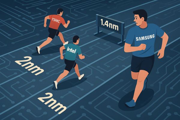
From a technological point of view, Intel 18A represents a truly significant innovation, especially when we consider that this process could bring the company back to the same level as TSMC's next-generation 2-nanometer technology. This shift in position could be significant not only from a technological perspective, but also from a geopolitical one, especially in a world where Taiwan's stability is increasingly in question. According to some capital market analysts, developments in the political situation in Taiwan – such as a Chinese “quarantine” scenario – could dramatically increase Intel's strategic value as an alternative semiconductor giant with a Western manufacturing chain.
Industry players are also following events with heightened attention. Intel is building several new factories in Arizona (Fab 52, Fab 62), while TSMC is also setting up its own facility there. The company's strategic goal is increasingly to not only manufacture its own products, but also to serve as a contract manufacturer for other companies – a kind of “Western TSMC”.
At the same time, the company's financial management has announced a stricter approach: they will only continue research and development on products that promise a gross profit margin of at least 50%. This more focused approach suggests that Intel is trying to reposition itself not only technologically, but also operationally.
Overall, Intel's 18A manufacturing technology is not revolutionary, but it is a serious and conscious step in a direction that could put the company on a more stable footing in the global semiconductor market in the long term. The success of the process will be determined not only by its technical parameters, but also by its practical applicability, industrial acceptance, and manufacturing economics. The coming period will also reveal how well the Panther Lake and Clearwater Forest processors can take advantage of the opportunities offered by the new platform – and whether this will be enough for Intel to truly return to the forefront of global technology.